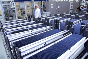
The Thin film industry is in constant evolution, enabling enhanced functionalities for technologically advanced devices such as:
- microelectronic devices
- wear resistant coatings and tribology
- optical coatings
- medical implants
- data storage media (e.g., CDs and DVDs)
- flat panel displays
- energy storage systems
- photovoltaic cells
- sensors
Thin film technology can be applied to different substrate materials such as metals, ceramics or polymers. Thin films are “grown” over substrates materials as glass, silicon, and steel. The deposition process and the material choice allows to improve properties of the substrate, enhanced functionalities.
The diverse technologies deposition available allow to deposit over flexible substrate, polymeric, organic or objects with very complex geometrical shapes.
Deposition materials for thin film processes can range from metals and pure elements to more complex compounds, such as oxides, nitrides and polymers. Source materials, in most cases, require high levels of purity to enable the desired functionality of the thin film coating. PhotonExport ensures raw materials comply to the required purity, typically 99,99% but ranging up to 6N or 99,9999% which are often required in Thin Films R&D and scientific applications.
The generally accepted industry definition of a “thin film” layer is one that is thinner than 5 microns. Layers thickness above eight microns is commonly called “thick films.”
The thin film can be form at the atomic or molecular level, a layer at the time (ate the angstrom level) as per the ALD or Atomic Layer Deposition technique. Depositions can occur in the vapor (Chemical Vapor Deposition) or solution state and be based on physical processes (Physical Vapor Deposition) involving high vacuum chambers, or chemical reactions.
According to the application, the substrate and material layer is structure by patterning by lithography and etching and also by multi patterning depositions phases. The device’s construction process, for example for Microelectromechanical systems (MEMs) is completed by finishing and packaging steps (such as assembly) which vary based on the type of device.
