ALD is a special adaptation of chemical vapor deposition (CVD) technique pioneering in semiconductor production and suitable for manufacturing inorganic material layers with a thickness down to a fraction of monolayers
A. M. Shevjakov
Atomic layer deposition (ALD) has gained a lot of attention as a thin film deposition method, as it is uniquely suitable for depositing uniform films on complex three-dimensional topographies. Compared to other chemical vapor deposition (CVD) techniques or physical vapor deposition (PVD) ALD furthermore has the particularity to control the thickness and composition of the deposited material at an atomic level. Therefore it is one of the revolutionary methods in the production of dielectrics in semiconductors that allow to reduce the chip size keeping Moore´s law. ALD is also a usual in electro optics, biomedical devices, photovoltaics and microelectronics and part of our Thin Films Process Equipment portfolio at PhotonExport.
The ALD concept
Behind this outstanding deposition performance is based on the ALD-cycle that consists out of 4 distinguished steps and relies on successive, separated and self-terminating gas-solid reactions. In the initial step a gas containing the desired material for deposition is flushed into the chamber with the sample inside. The reactant starts to build a uniform layer on all sides of the sample. As this gas-solid reaction is self-limited it terminates after all reactive sites on the sample surface are consumed.
In the second reactant that is flushed into the chamber in the third step. Comparable to the first reactant, that second reactant builds a uniform layer on all sides of the sample and terminates after all reactive sites on the first layer are consumed. Thereby a second layer is built on top of the first one. In the final step the chamber is purged or evacuated again to remove the non-reacted second reactant and the whole cycle starts again.
The sequential use of these self-terminating gas-solid reactions leads to an increasing number of layers and therefore an increasing thickness of the deposited material with a characteristic growth in every ALD-cycle. By selecting a specific number of ALD-cycles a control of thickness and composition can be reached at an atomic level.
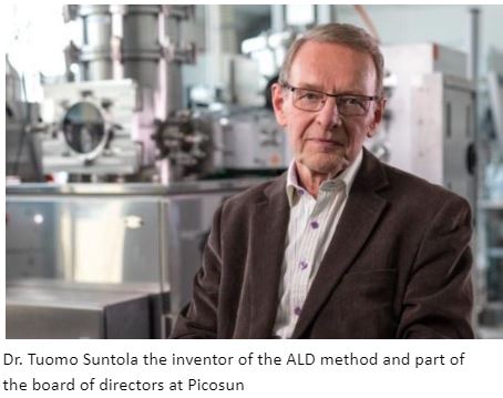
Earliest research on ALD was already done in the 1960s by the two scientists Stanislav Koltsov and Valentin Alteskovsky. Despite that the more commonly acknowledged scientific origin of ALD (at that time developed under the name “atomic layer epitaxy” ALE) was in the 1970s in Finland by Dr. Tuomo Suntola. Especially in the 1990s and the 2000s interest in ALD increased, as the first large-scale proof-of-concept of ALD-EL displays, manufactured using the ALD process, for flight information at Helsinki-Vantaa airport could be shown. Nowadays ALD is an essential element of the toolbox for processing materials at the atomic level especially in the semiconductor industry and the production of technical devices as displays or smartphones heavily relies on it.


Different ALD processes exist
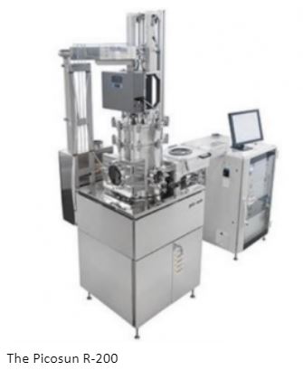
– for example Thermal ALD, Plasma ALD, Photo-assisted ALD and Metal ALD – which require different temperatures and make use of different kinds of precursors and different reaction times. All of them require a high substrate purity for good deposition characteristics, which specifically highlights the importance of substrates having the sufficient quality. We at PhotonExport are providing one of the global market leader systems in advanced ALD research from Picosun, which has Dr. Tuomo Suntola – the inventor of ALD – in its board of directors. The Picosun R-200 Advanced is capable of processing wafers with a diameter of up to 200mm, but also 3D objects. It has a possible processing temperature from 50 – 500°C, enables thermal and plasma ALD , is equipped with highly functional and easily exchangeable precursor sources and much more, which makes it the perfect ALD device for almost every kind of requirement.
| TECHNICAL FEATURES | |
| Typical substrate size and type | • 50-200 mm single wafers • 156 x 156 mm solar Si wafers • 3D objects • Powders ans particles • Mini-batch • Porous, through-porous, and high aspect ratio up to 1 :2500 |
| Processing temperature | • 50 – 500 ºC, plasma 450ºC (650ºC with heated chuck on request) |
| Typical Processes | • Al2SO3, TiO2, SiO2, Ta2O5, HfO2, ZnO, ZrO2, TiN, AIN, metals such as Pt or Ir |
| Substrate loading | • Manual loading with pneumatic lift • Load lock with magnetic manipulator arm • Semi-automatic loading with handling robot. • Cassette-to-cassette loading with cluster tools. |
| Precursors | • Liquid, solid, gas, ozone • Up to 12 sources with 6 separate inlets (7 if the plasma option is chosen) |
| Options | • Cluster tools, PicoflowTM diffusion enhancer, roll-to-roll chamber, RGA, ellipsometer (load lock tools), UHV compatibility, N2 generator, gas scrubber, customized designs, glove box integration for inert loading. |
1 A. M. Shevjakov, G. N. Kuznetsova, and V. B. Aleskovskii, in Chemistry of High-Temperature Materials, Proceedings of the Second USSR Conference on High-Temperature Chemistry of Oxides, Leningrad, USSR, 26–29 November 1965 Nauka, Leningrad, USSR, 1967, pp. 149–155, in Russian.
2 Ville Miikkulainen, Markku Leskelä, Mikko Ritala, and Riikka L. Puurunen , “Crystallinity of inorganic films grown by atomic layer deposition: Overview and general trends”, Journal of Applied Physics 113, 021301 (2013) https://doi.org/10.1063/1.4757907
3 Riikka L. Puurunen , “Surface chemistry of atomic layer deposition: A case study for the trimethylaluminum/water process”, Journal of Applied Physics 97, 121301 (2005) https://doi.org/10.1063/1.1940727
4 M. Ritala and M. Leskelä, in Handbook of Thin Film Materials, editedby H. S. Nalwa (Academic, San Diego, 2002), Vol. 1, pp. 103–159.
5 Ville Miikkulainen, Markku Leskelä, Mikko Ritala, and Riikka L. Puurunen , “Crystallinity of inorganic films grown by atomic layer deposition: Overview and general trends”, Journal of Applied Physics 113, 021301 (2013) https://doi.org/10.1063/1.4757907
6 Ville Miikkulainen, Markku Leskelä, Mikko Ritala, and Riikka L. Puurunen , “Crystallinity of inorganic films grown by atomic layer deposition: Overview and general trends”, Journal of Applied Physics 113, 021301 (2013) https://doi.org/10.1063/1.4757907
7 T. Suntola and J. Antson, U.S. Patent No. 4,058,430 (15 November 1977).
8 Synthesis of Doped, Ternary, and Quaternary Materials by Atomic Layer Deposition: A Review Adriaan J. M. Mackus, Joel R. Schneider, Callisto MacIsaac, Jon G. Baker, and Stacey F. Bent Chemistry of Materials 2019 31 (4), 1142-1183 DOI: 10.1021/acs.chemmater.8b02878
