WHAT IS RTP AND ITS APPLICATIONS?
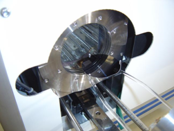
Rapid thermal processing, a major technique in semiconductor production, enables for faster processing of the silicon wafer by the use of high intensity lamps or lasers. To avoid thermal shock, the wafer is gently cooled. Dopant activation, thermal oxidation, metal reflow, and chemical vapor deposition are all examples of rapid thermal processes used in semiconductor production.
Rapid Thermal Processing was originally developed for ion implant annealing. In ion implantation, high energy ions deposited on the substrate by directly bombarding dopants into a substrate. While doing this process collision of the high energy ions with the atoms of the substrate causes changes and damages to the material structure of the substrate. Annealing heat treatment is applied to the material to restore the structure of the substrate prior to ion implantation. Although it was originally developed for this process, its applications have expanded to include oxidation, silicide formation, chemical vapor deposition, and advanced applications such as modifying the crystallographic phase of elements, compounds, or alloys to improve properties, lattice interface, or stress relaxation(https://photonexport.com/rapid-thermal-processing/).
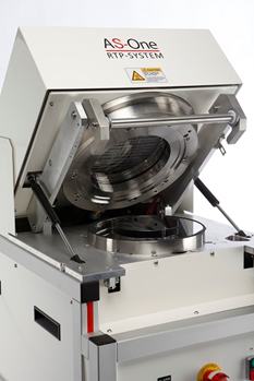
RTP is a dynamic technology that allows fast heating and cooling to process temperatures ranging from 200 to 1300°C, with ramp rates averaging 20 200°C/sec and good gas ambient control, allowing the creation of complex multistage processes within a single processing recipe.
Resident reactions processes
The first type of process is known as a resident reaction, in which heat is used to affect the structure of already existing materials in or on the wafer with no extra external materials. The following are applications of typical resident reactions: Implant annealing, Diffusion of dopants, Ohmic contact annealing, Thermal annealing of polymers, Densification and Crystallization.
Surface interaction processes
The second type of process is surface interaction, in which heat causes the wafer surface to be modified by gases distributed over it. The difference between the two categories is that during the heating process, material in the form of reactive gas is introduced. Following are a few examples: Oxidation, Silicon carbonization, Selenization, Nitridation.
The last type of Rapid Thermal Processing (RTP) is Rapid Thermal Chemical Vapor Deposition Process (RTCVD).
The deposition procedures of Rapid Thermal Chemical Vapor Deposition Processes (RTCVD) are based on Chemical Vapor Deposition (CVD). In CVD, gases react with the heated substrate’s surface to create a thin layer. Heat, photons, and plasma drive the chemical process.
In the semiconductor industry, pulsed technologies can be used to achieve more advanced results. PVD HIPIMS (high voltage energy – with a length of ~100 µs on the order of kW·cm-2), ultrashort pulse laser (femtosecond lasers) and now also RTP.
ANNEALING IN PULSE MODE
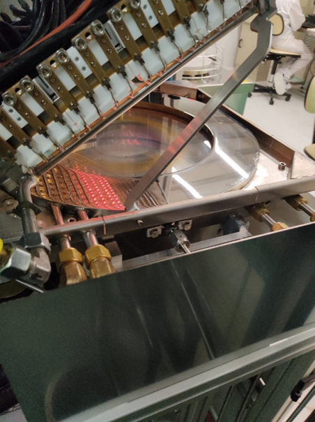
With the capacity to operate under vacuum, decreased pressure, secondary vacuum, and a broad temperature range, Annealsys enhances the capabilities of its quick annealing furnaces.
To anneal layers that are deposited on thermally sensitive substrates, Annealsys has created a pulsed annealing mode in response to client requests.
The Annealsys RTP system’s pulse mode allows for the generation of power pulses with a precision of 10 ms. Due to the halogen lamps’ response time, power pulses are typically in the 1 second range. Despite the fact that the operation is performed in an open loop, the power converters particularly designed to power the lights give remarkable consistency. This allows this annealing mode to be used in production for several years.
The following power pulse parameters can be configured: Ramping time, Starting power level, Ramp down of the pulse, High power of the pulse at the end of the ramp.
This allows for a background temperature (for example, 400°C) to be set and a power pulse to be generated starting from that temperature. The pyrometer can eventually control the pulses.
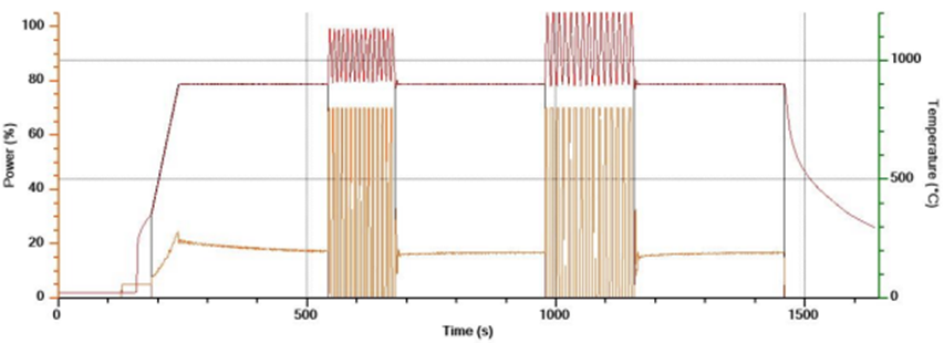
Controlling the power and duration of the pulses allows you to control the pulse energy from 5 to 100 Joules per pulse. The system allows for extremely precise adjustment of the power and energy of the pulses.
The power pulse energy is tuned to the same level as in a fast annealing system using flash lamps.
The preheating temperature can be controlled within the machine’s temperature range with a ±1°C precision.
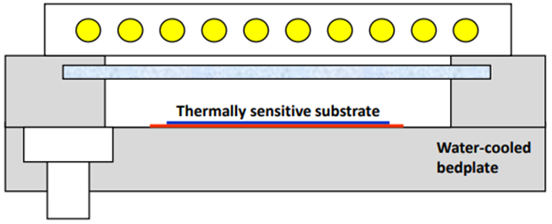
The machine also has the capacity to chill the substrate from rear while being heated from the top using Annealsys cold wall furnace technology, which creates a gradient of several hundred degrees between the two substrate sides. It is illustrated in the image below.
It is possible to create pulses with duty cycle ranging from 1 to 2 seconds.
Wavelengths range from visible to 4 mm.
Due to the power control of the lamps via special power converters, consistent exposure uniformity with great repeatability is achieved.
The Annealsys RTP system can anneal wafers installed on standard quartz pins as well as smaller pieces installed on a susceptor.
Annealsys can offer to run demo samples in its laboratory.

