PhotonExport a specialist in thin films and nanotechnology supplies, offers a wide range of Rapid Thermal Processing (RTP) and (RTA) equipment in Spain and Portugal.
Annealsys Rapid Thermal Processing (RTP) Systems
Annealsys Rapid Thermal Processing (RTP) furnaces can address various applications with an extended temperature range and vacuum capability. The infrared lamp furnaces can perform annealing up to 1450°C and for duration up to 1 hour at 1200°C. These versatile RTP systems can process samples from few mm² up to 200 mm diameter with manual loading or cassette to cassette robot handling for production, including customized solutions for processing compound semiconductor wafers with susceptors.
View more information about our offerings, or to get a Rapid Thermal Processing price quote use the form below.
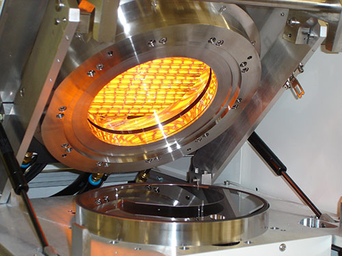
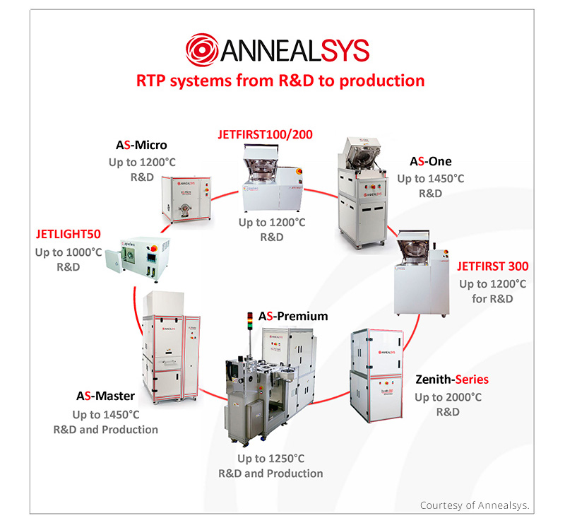
Annealsys AS-MICRO
The most powerful 3-inch rapid thermal processor for universities.
The AS-Micro is a compact table top three-inch rapid thermal processor with vacuum capability dedicated to research applications. It can process substrates from few square millimeters up to 3-inch diameter or square. Optional susceptors are available to hold small samples and to process substrates with low infrared absorption.
The quartz tube process chamber with stainless steel flanges and tubular infrared halogen lamps furnace allows running processes up to 1250°C with very fast ramp rates (> 250°C/s). The state of the art temperature controller provides accurate temperature control. The horizontal motion door with quartz tray provides easy access for loading and unloading of the wafers and thermocouple installation.
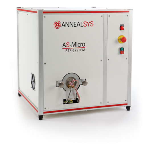
Annealsys AS-Micro Key Features:
- Infrared halogen tubular lamp furnace with silent fan cooling
- Quartz tube chamber with water cooled stainless steel flanges
- Fast digital PID temperature controller
- Thermocouple control (optional pyrometer)
- Atmospheric and vacuum process capability
- One purge line and up to 5 process gas lines with digital MFC
- PC control with Ethernet communication for fast data logging
- Optional SiC coated graphite susceptor for small samples
- Optional turbo pump and pressure control
- Optional double chamber for cross contamination issues
Annealsys AS-Micro Applications:
- Implant annealing
- Ohmic contact annealing
- Rapid Thermal Oxidation (RTO)
- Rapid Thermal Nitridation (RTN)
- Densification and crystallization
- Selenization
- CVD of graphene
- and more.
Request a quote or more information about the AS-MICRO System
More InformationAnnealsys AS-One
The AS-One RTP system is available for processing up 100 mm or up to 150 mm diameter substrates.
The Annealsys AS-One system is available with two sizes of reactors to process substrates up to 100 mm (4”) or 150 mm (6”) diameter. The machine has been specially developed to meet the requirements of research laboratories and small-scale production. The high reliability guarantees low cost of ownership. The floor standing configuration and the reduced footprint allow easy installation in cleanroom and easy access for maintenance.
The AS-One system has a stainless steel cold wall process chamber for better process reproducibility and higher cooling rates. The special design of the process chamber provides a low volume for fast pumping and purging and low consumption of process gases. Pyrometer and thermocouple temperature measurements are standard features.
The fast digital PID controller provides accurate and repeatable thermal control across the temperature range. The clam shell style design of the process chamber enables full access to the bedplate and easy access for loading and unloading the substrates as well as a practical cleaning of the chamber.
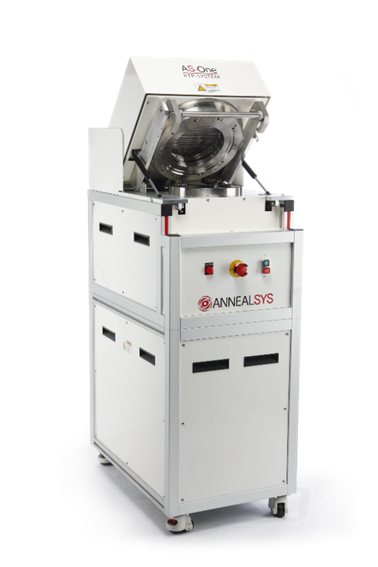
Annealsys AS-One Key Features:
- Infrared halogen tubular lamp furnace with silent fan cooling
- Stainless steel cold wall chamber technology
- Fast digital PID temperature controller
- Thermocouple and pyrometer control
- Atmospheric and vacuum process capability
- Purge gas line with needle valve
- Up to 5 process gas lines with digital MFC
- PC control with Ethernet communication for fast data logging
- Optional turbo pump and pressure control
Annealsys AS-One Key Applications:
- Implant annealing
- Ohmic contact annealing (III-V and SiC)
- Rapid Thermal Oxidation (RTO)
- Rapid Thermal Nitridation (RTN)
- Selenization (CIGS solar cells)
- CVD of graphene
- Silicon carbonization
- Sol-gel densification and crystallization
- Diffusion from spin-on dopants
- and more.
Request a quote or more information about the AS-ONE System
More InformationAnnealsys AS-Master
RTP system excellent for production applications.
The AS-Master is an ideal RTP system for production applications that require a cassette-to-cassette loading system. The manual loading version can be used to develop different processes.
The Annealsys AS-Master Rapid Thermal Processor is a flexible equipment that can perform a variety of processes ranging from annealing to Rapid Thermal Chemical Vapor Deposition. The high temperature version can perform annealing operations up to 1450°C and enables for the development of new processes.
Cold wall chamber technology ensures excellent process repeatability in a contamination-free environment. AS-Master is appropriate for a wide range of RTP and RTCVD operations because to its increased temperature range, vacuum performance (atmosphere to 10-6 Torr), and gas mixing capacity.
For increased process environment cleanliness, loadlock and cluster tool module versions are offered. Manual loading and cassette-to-cassette versions make the system suited for process research and simple production transfer.
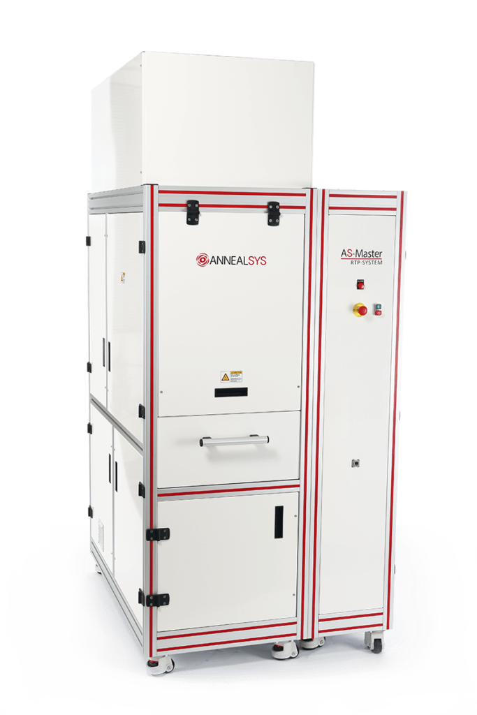
Annealsys AS-Master Key Features:
- Multi-zone infrared halogen lamp furnace with close loop air cooling
- Stainless steel cold wall chamber technology
- Fast digital PID temperature controller
- Thermocouple and pyrometer control
- Atmospheric and vacuum process capability
- Up to 8 process gas lines with digital MFC and one purge gas line
- PC control with Ethernet communication for fast data logging
- Gas panel for standard or hazardous gases
- Optional turbo pump and downstream pressure control
- Manual or cassette to cassette loading
Annealsys AS-Master Applications:
- Implant annealing
- Ohmic contact annealing (III-V and SiC)
- Silicon carbonization
- Rapid Thermal Oxidation (RTO)
- Rapid Thermal Nitridation (RTN)
- Diffusion from spin-on dopants
- Densification and crystallization
- Selenization
- Rapid Thermal CVD
- Thermal annealing of polymers
- and more.
Request a quote or more information about the AS-MASTER System
More InformationJETFIRST 200
Ideal for R&D applications from MEMS to SOLAR
Request a quote or more information about the JETFIRST 200 System
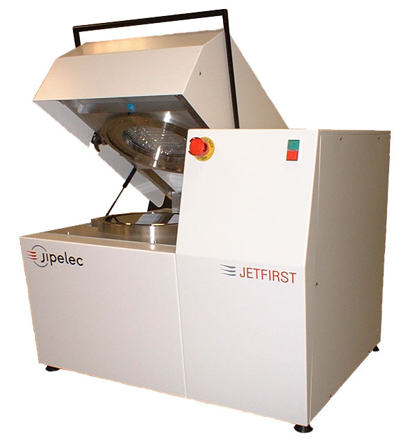
More InformationThe JetFirst 200 system is a cost-effective bench-top RTP processor ideal for R&D applications from MEMS to SOLAR. The system includes a cold-wall reaction chamber, a powerful infrared lamp furnace, and a software that allows full process monitoring, data acquisition and pyrometer calibration for a large range of substrates.
JetFirst 200 Key Features:
- Temperature range: from room temperature to 1450°C (depending upon version)
- Up to 200°C/s ramp rate (depending upon version)
- Capability for gas mixing using mass flow controls
- Manual or automatic substrate loading
- Atmosphere to 10-6 Torr vacuum range
JetFirst 200 Applications:
- Rapid thermal annealing (RTA)
- Rapid thermal Oxidation (RTO)
- Nitridation (RTN),
- Rapid Thermal Diffusion from spin-on dopant
- Crystallization
- Contact Alloying
- Solar applications for PV industry
- and more.
JETLIGHT 50 – RTP SYSTEM
Designed to meet requirements of R&D laboratories and small-scale production.
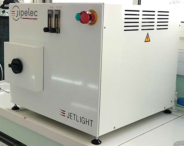
The JetLight50 system is a a versatile, compact size and cost effective, software controlled bench-top type RTP tool, specifically designed to meet requirements of R&D laboratories and small-scale production units.
JetLight 50 Key Features
- Software-controlled (PLC and PC)
- Hot-wall (quartz tube) chamber design
- 2 gas lines with manual ball flow meter control
- Substrate size up to 50mm diameter
- Quartz tubes substrate holder
- Atmospheric and vacuum process capabilities
- Microprocessor-based thyristor technology
JetLight 50 Applications
- Rapid thermal annealing (RTA)
- Rapid thermal Oxidation (RTO)
- Nitridation (RTN), Diffusion (RTD)
- Implant monitoring
- Cystrallization
- Carbonization
- Contact alloying
- and more.
Request a quote or more information about the JETLIGHT 50 System
More InformationRequest your tailored Rapid Thermal Processing price quote today and explore our solutions designed to elevate your research and production needs. Our dedicated team ensures you receive detailed pricing information, enabling informed decisions about our high-performance RTP equipment. Don’t miss out on the opportunity to enhance your operations with our advanced technology. Get your Rapid Thermal Processing price quote now!
