Silicon Wafer & Crystal

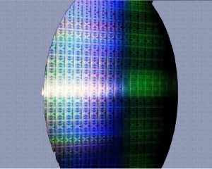
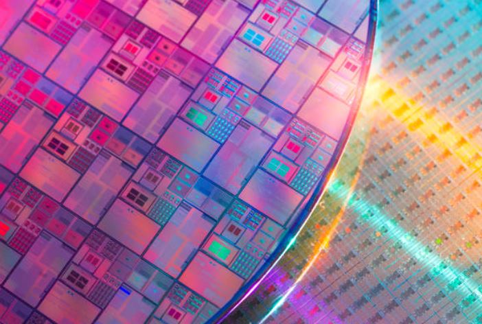
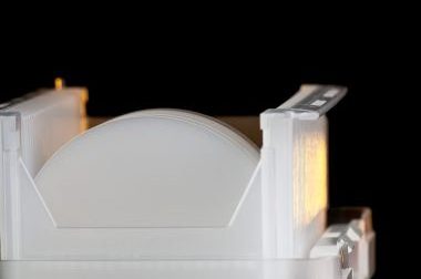
Silicon wafer

Silicon wafers

PhotonExport supplies small quantity silicon wafer and crystal as detailed below.

Specifications:

Choose from the specifications listed below. We have no minimum order quantity.

  • SSP: Single-Side Polished
  • DSP: Double-Side Polished
  • Thickness form the Super-Thin 2 micron wafer up to thick wafer or ingo
  • Doped P, Doped N or Undoped
  • Select your standard orientations per example (100) or (110) or (111). Check with us for your specific orientation to ensure suitable results

Available Diameters

25.4 mm Si Wafer,  50.8 mm Si Wafer, 76.2 mm Si Wafer, 100 mm Si Wafer, 125 mm Si Wafer, 150 mm Si Wafer, 200 mm Si Wafer, 300 mm Si Wafer, 450 mm Si Wafer

Thermal Oxide Silicon Wafers

Thermal Oxide (SiO2)

Diameter ranging fom 25.4 mm to 300 mm

Thickness available from 200 Angstroms (Å) to 15 µm

Silicon Nitride Wafers

Stoichiometric LPCVD (low-pressure chemical vapor deposition) Silicon Nitride  wafer

PECVD (Plasma enhanced chemical vapor deposition) Silicon Nitride wafer (deposited at low temperatures)

Commonly supplied for your integrated photonics application

SILICON CRYSTAL WAFERS1Indium Gallium Arsenide Wafers

We supply single crystal InGaAs

InGaAs is principally used for infrared detectors. Other applications include avalanche photo diodes, some of the fastest transistors, and photovoltaic triple-junction

Commonly supplied for your integrated photonics application

Indium Phosphide wafers

Diameters available: 2″, 3″

For your integrated photonics application

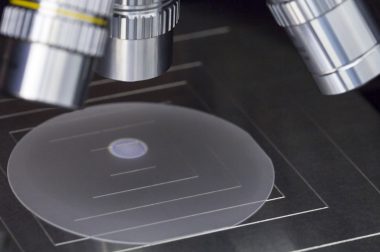
Crystal Wafers

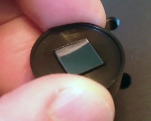
LiNbO3 waferSpecifications

Choose your orientation

(100), (001), (111), (110) for cubic and tetragonal crystals

(0001), (1102), (1120), (1010) for hexagonal crystals

Other orientations are available with higher Miller index values or vicinal substrates

Orientation accuracy : ± 0.5°, typical < 0.3°, or better on request

Choose your standard size:

5 mm x 5 mm, 10 mm x 10 mm, 10 mm x 5 mm, 15 mm x 15 mm

12,7 mm x 12,7 mm, 20 mm x 20 mm, 25 mm x 25 mm, ø1″, ø2″

Lateral tolerances:

+0/-0.05 mm

Standard thickness:

0.5 mm, 1.0 mm, other thicknesses down to 0.1 mm on request

Vertical tolerance:

+/- 0.05 mm, or better on request

Polishing:

One or both sides epi-polished (epitaxy ready polished)

Surface quality: scratch free under magnification 50x

Micro-Roughness (measured with interferometer microscope)
(lateral resolution : 0.65 µm, theoretical vertical resolution from 0.01 nm)
Roughness: ( λcut off =0.08 mm)
Ra: < 0.5 nm
Rq: < 1.0 nm
Rt: < 2.0 nm

Crystals usually in stock:

Aluminum, CeO2, GdScO3, LiF, PbSe, Tb-Dy-Fe (GMM), Al2O3 (sapphire), CdS, GGG, MgAl2O4 (spinel), PbTe, W (Polycrystal), AlN, CdSe, Graphite, Mg, SrTiO3, WS2, Ag, CdTe (HgCdTe), InAs, MgF2, Nb:SrTiO3, WSe2, Au, CdZnTe, InP, MgO, SrLaAlO4, WTe2, Au/Cr coated, SiO2/Si, CsI (TI), InSb, Mica Disks, SrLaGaO4, BaF2, DyScO3, KCl, Mo (Polycrystal), SiO2 (quartz), YAlO3 (YAP), BaTiO3, Diamond, KH2PO4, MoS2, SiC (4H, 6H, 3C), YAG, Bi2Se3, Diamond Epi Film on Si, KTN, MoSe2, SBN, YIG, Bi2Te3, Fe (SS-Poly), KTaO3, MoTe2, Si, YVO4, Bi4Ge3O12(BGO12), Fe2O3, LaAlO3, NaCl, Si-Ge, YSZ, Bi12GeO20(BGO20), Fe3O4, LaF3, NaBi(WO4)2, SOI, ZnO, BN (h), Ga2O3-ß, La3Ga5SiO14, NdCaAlO4, SOS, Black Phosphorus, GaAs, LiAlO2,  Nickel (single xtl), Ti (polycrystal), ZnS, CaF2, GaN, LiGaO2, NdGaO3, TiO2(Anatase), Zn, C (single crystal), GaSe, LSAT, PBN, TiO2 (Rutile), ZnSe, CaCO3 (Calcite), GaP, Li, PET Film, Ta, ZnTe, Cu, GaTe, LiNbO3, PbWO4, TGG, Zr, Ce: Lu2SiO5, GaSb, LiTaO3, PMNT, TeO2, Zero Diffraction Plate, CdWO4, Ge, Lu2SiO5: Ce, PbS, TbScO3, Two Dimensional Crystal.

If you can´t find it in our listing, ask us for more and custom solutions.

Ceramic Wafers:

PhotonExport provides Alumina substrate (Al2O3),  Zirconia substrate (ZrO2) and Aluminum Nitride substrate (AlN).

Al2O3 substrate has a very communused due to its excellent high mechanical strength and very high heat resistance. Properties includes a very small dieletcric loss which makes alumina substrates very good for high-performance microelectronic packaging. Its high abrasion resistance make Al2O3 a good performer as a grinding media. The surface of alumina substrate is quite smooth and low porosity, 99.6% alumina substrate is suitable for thin film device, 96% alumina substrate is suitable for thick film device application.

DescriptionAl2O3 Wafer Type 1Al2O3 Wafer Type 2Al2O3 Wafer Type 3Al2O3 Wafer Type 4
Purity (wt%)0.9699.6%99.6%99.9%
Density (g/cm3)> 3.753.883.873.92
Thermal conductivity (W/m. K)2434.73535
Thermal Expansion (x10-6/oC)< 7.77~8.37~8.38.1
Dielectric Strength (Kv/mm)> 1423.6423.648.7
Dielectric Constant (at 1MHZ)9.89.99.99.8
Loss Tangent (x10-4 @1MHZ)411< 1
Volume Resistivity (ohm-m)> 1013 @ 20 Cº; > 3x10⁷ @ 500 Cº> 1014 @ 25 Cº; > 109 @ 500 Cº> 1014 @ 25 Cº; > 1010 @ 500 Cº> 1015 @ 25Cº; 1012 @ 500 Cº
Flexural Strength (N/mm2)>330593621400
Surface Roughness (micron)as fired 0.3 as lapped 0.075 as polished 0.025