Photon Export is a key player in providing cutting-edge equipment and materials for semiconductor fabrication in Spain and Portugal. Our expertise in nanofabrication allows us to offer not only top-notch equipment and materials but also comprehensive consulting and educational services. With our broad team of international consultants, we provide tailored guidance and training programs for front end semiconductor manufacturing processes, designed to address the specific needs and challenges of new clean room projects or ensuring you stay at the forefront of technological advancements and industry best practices in nanofabrication.
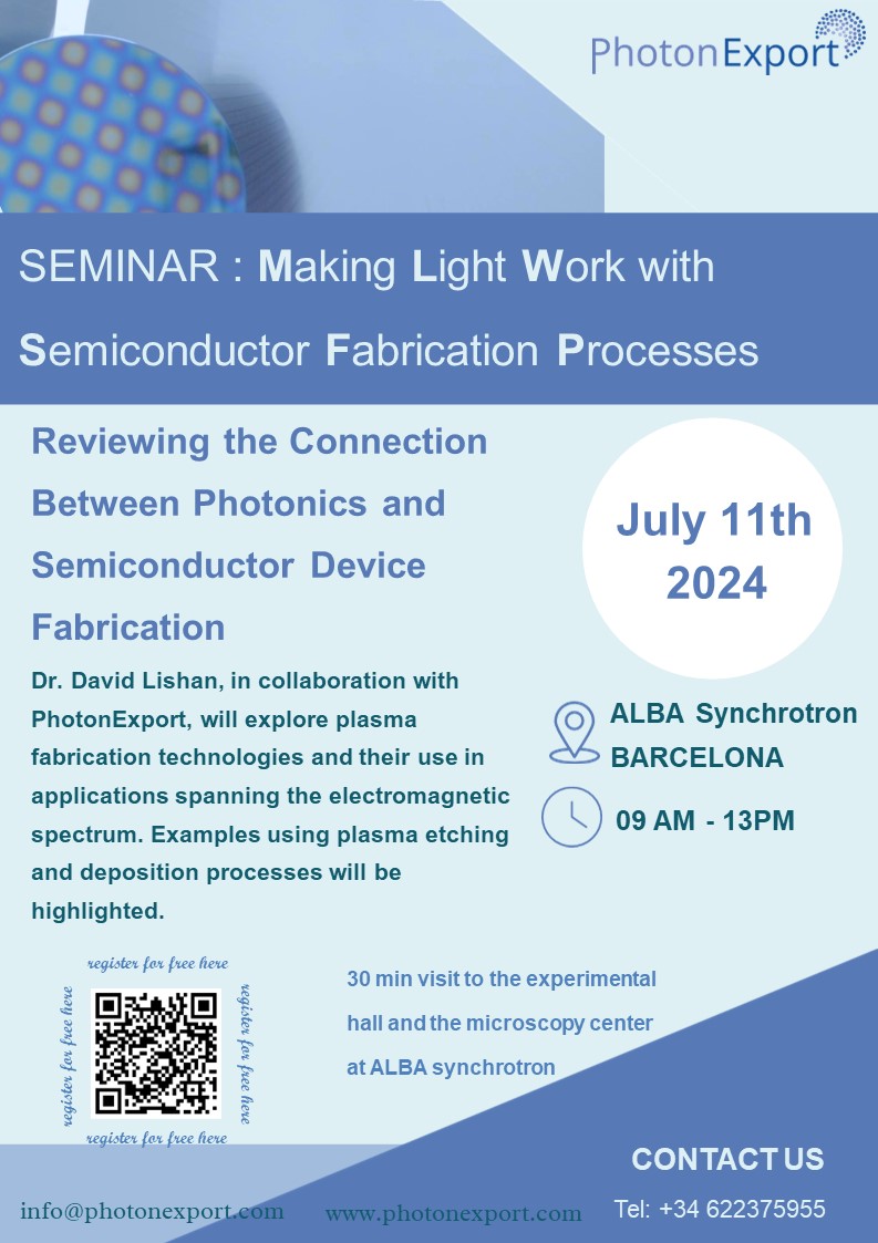
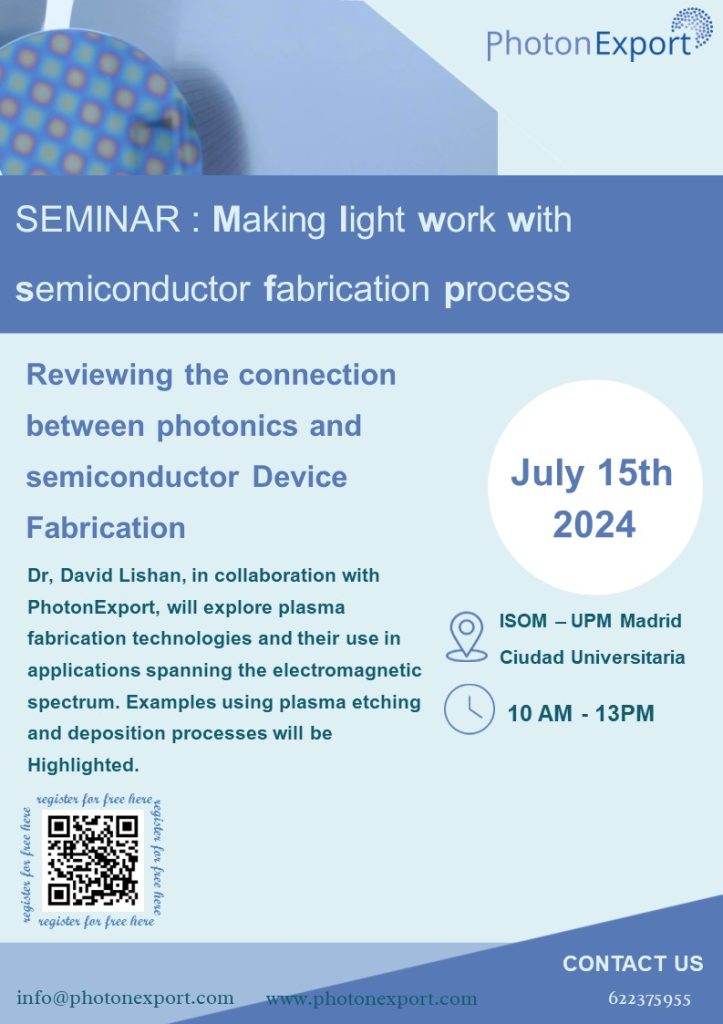
On July 11, 2024, at the ALBA Synchrotron in Barcelona, and on July 15, 2024, at 10:00 AM at the ISO at the Universidad Politécnica de Madrid (Ciudad Universitaria), we will briefly introduce you to our capabilities and advanced solutions for nanofabrication. We will then, in a 3 hours talk, explore plasma fabrication technologies and their use in applications spanning the electromagnetic spectrum. Examples using plasma etching and deposition processes will be
Highlighted.
we will go . These events are a great chance to learn about our offerings, share knowledge, and network with industry peers. We have prepared in-depth discussions on two main processes related to depositions and dry etching.
Thank you for joining us. We look forward to engaging with you throughout this seminar and exploring the future of innovation together.
Register for free Barcelona 11th july 2024 9:00 am Seminar https://indico.cells.es/event/1535/

Register for free for Madrid 15th july 10:00 am 2024 Seminar https://forms.gle/fLSWNqq6QJrtGL7v5

After receiving an undergraduate degree in Chemistry from UC Santa Cruz and Ph.D. from UC Santa Barbara in Solid State Electrical Engineering Dr. Lishan worked and published on a wide range of material, semiconductor, and chemistry R&D projects in the areas of lithography, photochemistry, x-ray mask fabrication, PVD, and plasma processing. During over 25 years at Plasma-Therm, he had business unit management and worldwide technical marketing responsibilities as well as leading the development and release of the plasma dicing system.

After receiving an undergraduate degree in Chemistry from UC Santa Cruz and Ph.D. from UC Santa Barbara in Solid State Electrical Engineering Dr. Lishan worked and published on a wide range of material, semiconductor, and chemistry R&D projects in the areas of lithography, photochemistry, x-ray mask fabrication, PVD, and plasma processing. During over 25 years at Plasma-Therm, he had business unit management and worldwide technical marketing responsibilities as well as leading the development and release of the plasma dicing system.
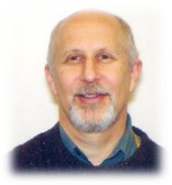
David Lishan, Ph.D.
He has presented plasma processing workshops at leading institutions throughout the world, including Harvard University, UC Berkeley, University of Notre Dame, UC Los Angeles, University of South Florida, Stanford University, Lund University, IMRE, UC Santa Barbara, ISCAS, SINANO, Shanghai Jiao Tong University, UT Austin, Cornell University, Pennsylvania State University, KANC, University of Alberta, Weizmann Institute, University of Queensland, University of New South Wales, Politecnico di Milano, International Iberian Nanotechnology Laboratory, Institute of Microelectronics of Barcelona and many others.
