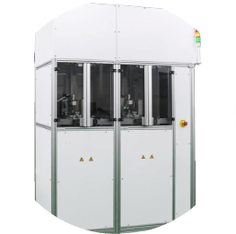
It is a solution-based process used for the fabrication of thin films, in the thickness range from micrometre to nanometre, to deposit uniform coating of organic materials on flat surfaces.
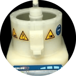
Rapid thermal processing
Describes a class of techniques that provide a way to rapidly anneal wafers to elevated temperatures for relatively short times. These processes have a wide variety of applications in semiconductor manufacturing.
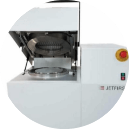
PECVD horizontal furnace
Horizontal Tube Furnaces allow the synthesis of a wide variate of materials in either gaseous, vapor, liquid and solid sources.
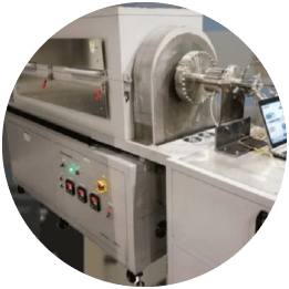
Reactive Ion Etching
Reactive ion etching is a process thatr removes materials chemically from substrates using ion bombardment. The main advantages of using this process are that it provides directional etch while being much stronger than isotropic plasma.
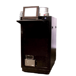
Ion Beam Milling
Ion Beam Milling is a process consisting of a direct beam of ions inciding at a substrate in a vacuum chamber. It is based on the momentum exchange between incident ions and atoms of the target material in the collision.
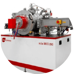
PECVD vertical furnaces
This company offers two different models of compact batch- type, single or multichambered furnace. They provide high precision semiconductor processing as well as a wide range of operating pressures.

Contact us and ask for information
¡¡ Opening up the Thin Films Equipment Market !!
PhotonExport, experts in Sputtering Targets, Silicon, Sapphire and crystals substrates, consolidates his strength in the thin film value chain by partnering with leading Equipment Manufacturers
Ask for informationPhotonExport supplies the best equipment for high quality and grade thin films
Vacuum Evaporation
Vacuum evaporation is a typical method used for deposition of functional films on to various substrates.
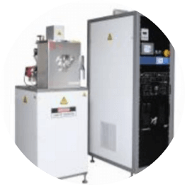
Vacuum Magnetron Sputtering
Magnetron sputtering is a high-rate vacuum coating technique that allows the deposition of many types of materials, including metals and ceramics.
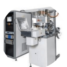
Atomic layer deposition
ALD process consists of thin film growth by consecutive atomic layers. ALD is the most advanced technique in thin film coating due to the precise control of film thickness (nm) it offers.
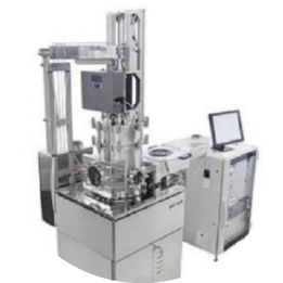
Spin coating
It is a solution-based process used for the fabrication of thin films, in the thickness range from micrometre to nanometre, to deposit uniform coating of organic materials on flat surfaces.

Rapid thermal processing
Describes a class of techniques that provide a way to rapidly anneal wafers to elevated temperatures for relatively short times. These processes have a wide variety of applications in semiconductor manufacturing.

PECVD horizontal furnace
Horizontal Tube Furnaces allow the synthesis of a wide variate of materials in either gaseous, vapor, liquid and solid sources.

Reactive Ion Etching
Reactive ion etching is a process thatr removes materials chemically from substrates using ion bombardment. The main advantages of using this process are that it provides directional etch while being much stronger than isotropic plasma.

Ion Beam Milling
Ion Beam Milling is a process consisting of a direct beam of ions inciding at a substrate in a vacuum chamber. It is based on the momentum exchange between incident ions and atoms of the target material in the collision.

PECVD vertical furnaces
This company offers two different models of compact batch- type, single or multichambered furnace. They provide high precision semiconductor processing as well as a wide range of operating pressures.
