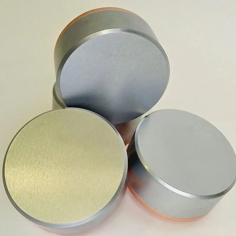
Sputtering target is a physical vapor deposition (PVD) process to form thin films. Thickness of layer formed varies from a few nano-meters up to several microns.
Sputter PVD consist of collisions of ions in vacuum and a plasma environment under strong magnetic field in order to extract atoms from the target and gradually grow a thin film over the desired substrate.
Scientific researchers generally use small discs (typical diameters ranges from 0.25 to 2, 3 or 4 inches) as sputter targets.
Nonetheless, myriad of targets shapes are possible, such as small cylinders, hollow tubes (rotatable targets) and long plates according to the industrial application and the continuous or batch deposition process. Powder metallurgy is the common process to manufacture most targets.
Sputtering Target: uses & manufacturing process
Even though Grove and Faraday first reported the sputtering phenomenon, it was Edison who managed to file the first patent in 1884, pertaining to a sputtering process by arc deposition and thermal evaporation method from a solid surface. Today microelectronics, photovoltaic, optics, metal and tribology sectors all make use of PVD thin film deposition.
Sputtering target materials
At PhotonExport, we offer a premier range of sputtering target materials. Our collection includes high-purity metals like Aluminum, ranging from 99.99% to 99.9999% in purity, to Antimony with purities of 99.999- 99.99999%, and more.
Beyond metals, our diverse alloy selection showcases combinations such as Aluminum-Chromium (AlCr) at 99.99%, and much more. We also provide specialized materials, from antimonides like Gallium Antimonide (GaSb) to selenides, silicides, sulfides, and tellurides.
View our wide selection of sputtering targets today: PhotonExport Sputtering Targets

