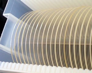
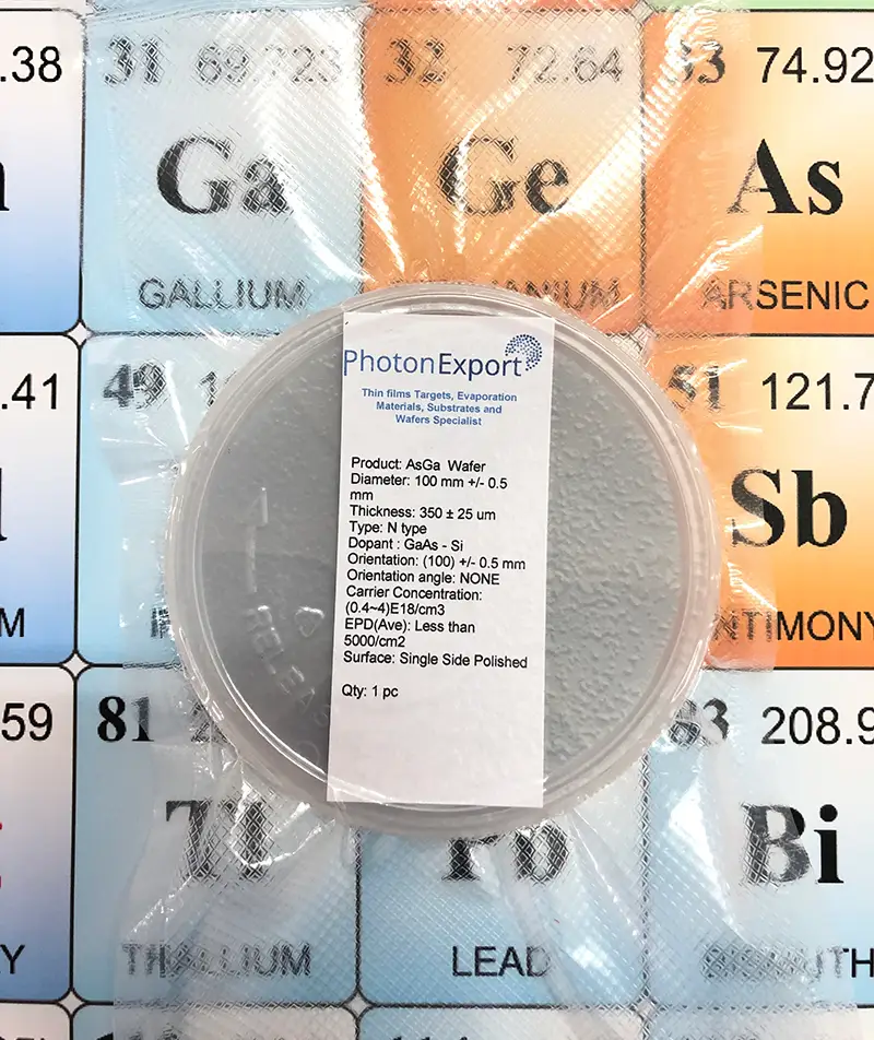
Welcome to PhotonExport, the leading provider of high-quality Crystal Wafers for the scientific and technological community. Our precision-cut wafers are the foundation for innovations across the semiconductor, photonics, and nanotechnology industries.

Choose Your Crystal Wafer Orientation
We offer a wide range of orientations to suit your specific needs:
- Cubic and Tetragonal Crystals: (100), (001), (111), (110) orientations
- Hexagonal Crystals: (0001), (1102), (1120), (1010) orientations
- Additional high Miller index values or vicinal substrates available upon request.
Our orientation accuracy stands at ± 0.5°, typically < 0.3°, with even finer precision available on request.
Crystal Wafers Standard Sizes to Fit All Requirements
Select from our standard wafer sizes to match your project specifications:
- Square dimensions from 5 mm x 5 mm, 10 mm x 10 mm, 10 mm x 5 mm,
15 mm x 15 mm,12,7 mm x 12,7 mm, 20 mm x 20 mm, 25 mm x 25 mm - Round wafers available in ø1″ and ø2″
- Custom sizes and shapes available to ensure the perfect fit for your application. Contact us for details.

Crystal Wafer Tolerances
- Lateral Tolerances: contact us for details.
- Standard Thickness: contact us for details.
- Vertical Tolerance: contact us for details.
Superior Polishing for Optimal Performance
- Epi-polished: One or both sides polished to epitaxy-ready standards
- Surface Quality: Scratch-free under 50x magnification
- Micro-Roughness: Measured with interferometer microscope for ultimate smoothness
(lateral resolution: 0.65 µm, theoretical vertical resolution from 0.01 nm)

Custom Solutions for Unique Challenges
Can’t find what you’re looking for? Our team specializes in providing custom solutions and wafer crystal orientations to meet the most challenging requirements. Contact us today for personalized assistance.
