Soda lime glass or silica sand based standard glass represents 90% of glass offering. To form borosilicate glass we need to add boric acid (B2O3), alumina and soda ash to the silica melt. Low thermal expansion (3,3 × 10⁻⁶ K−1 ) is the main property of Borosilicate glass According to the SiO2 content and alkaline earth content there are three groups of borosilicate glass. The Non-alkaline-earth borosilicate glass group or borosilicate 3.3 has around 12% B2O3. The Alkaline-earth-borosilicate glasses group has less boric acid and SiO2 content and 5% of alkaline earth and/or alumina like the Aluminoborosilicate glass. The High-borate borosilicate glasses contain 15 to 25% of B2O3, 65% to 70% of SiO2, and smaller amounts of alkalis and alumina and have low softening points and low thermal expansion but reduce chemical resistance.

Photon Export proposes all borosilicate type of glass substrates from world leaders in specialty glass as Schott, Corning, GE, Ohara, Hearaus and HOYA. Any shapes, cuts and polishing specifications are made: from standard squares, to Silicon wafers or optical components for the photonics scientific researcher.
Fused Silica, Silicon wafer, Sapphire crystal or other monocrystalline or polycrystalline crystals completes the substrates portfolio.-Substrates Soda Lime or Borosilicate Glass, Wafers and Crystals
Evaporation Materials for Physical vapor deposition
PhotonExport high purity metals, oxides, rare earths and compounds are processed, refined and purified from raw material to achieve science requirements and technological applications highest standards. Clean-room facilities, muffle or tube furnaces and precision characterization equipment ensure grades for semiconductor, electronic, deposition, fiber optic, and MBE (Molecular Beam Epitaxy) are met (up to 99, 9999%).
The most common processes to form thin films layers are Thermal evaporation and electron-beam evaporation. The thermal pvd (physical vapor deposition) has the benefit of a simple implementation and to consume small quantities of materials, very valuable for precious metal deposition. The high energy of electron beam process allows evaporation of ceramic oxides. It has become a standard in the ophthalmic industry to form the anti-reflection AR coating over glass, CR9 or other polycarbonate lenses.-Vacuum Evaporation Materials
Sputtering Targets: use & manufacturing process
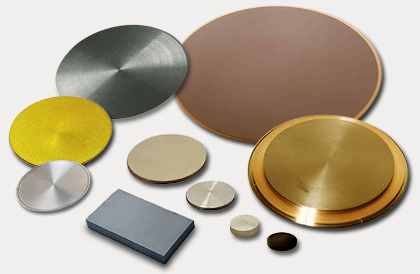
Sputtering is a physical vapor deposition (PVD) process to form thin films. Thickness of layer formed varies from a few nano-meters up to several microns. Sputtering PVD consist of collisions of ions in vacuum and a plasma environment under strong magnetic field in order to extract atoms from the target and gradually grow a thin film over the desired substrate. Scientific researchers generally use small discs (typical diameters ranges from 0.25 to 2, 3 or 4 inches) as sputtering targets. Nonetheless, myriad of targets shapes are possible, such as small cylinders, hollow tubes (rotatable targets) and long plates according to the industrial application and the continuous or batch deposition process. Powder metallurgy is the common process to manufacture most targets.
Even though Grove and Faraday first reported the sputtering phenomenon, it was Edison who managed to file the first patent in 1884, pertaining to a sputtering process by arc deposition and thermal evaporation method from a solid surface. Today microelectronics, photovoltaic, optics, metal and tribology sectors all make use of PVD thin film deposition.-Sputtering Target: use and manufacturing process
